3D ASSEMBLY AND VERIFICATION GUIDELINES, FOR PCB DESIGNS
When we are developing an electronic project and we are at the point where we want to enter the exterior design stage of our product, such as a box for prototyping, we can interact the 3D model of the chosen box with our electronic design (PCB).
This is done in order of observing the fixing points of the card, power connection inputs, sensor inputs, cooling and dissipation stages, on and off connections, internal height dimensions of the components assembled on the card plus more variables regarding the height dimensions of the boxes, and many more that must be taken into account. To do this I use the Altium designer import design tools, in which we will talk in more detail on the following image.
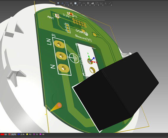
Figure 1. PCB Board Assembly with 3D box model
In the previous example, we can see the integration of the 3D models of our final product, as well as we can verify that the dimensions of our box are in accordance with the design of our PCB board, with this we can correct possible lags, errors that occur at the time to do the integration; This is an essential tool when the assembly is very complex, and we need to integrate several cards and 3D bodies, such as a voice assistant, a laptop, in addition to this, in Altium we can integrate 3 components, such as box models 3D, electrical connections of each track of our card, dimensions of the different characteristics of the PCB card, in order to verify functionality and assembly of our final product.
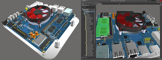
Figure 2. Altium Designer MiniPC project, example of 3D model integration.
This tool is very important since it allows the development of highly complex electronic products, and therefore each stage of the development of said product must be analyzed in detail, in order to minimize the chances to make the slightest mistake, shorten delivery times, among other things, this tool is very useful for designers when developing professional products.
keep around, I have planned a complete series for hardware and PCB design basics and tips.
Make sure to follow me on Linkedin
https://www.linkedin.com/in/danilo-gil-ortega-6006b7b4/
and Lya Electronic
https://www.linkedin.com/company/lya-electronic-corp/?viewAsMember=true
Posted by

Danilo Ortega – Electronic Engineer