Altium designer, using the Connection Verification Tool
When designing a PCB (printed circuit board), it is very important to verify each of the connections in our circuit, to corroborate different parameters such as the clearance between tracks, voltage lines, track width, microns, all this in order to visualize and verify our connections, we can visualize this in 3D and 2D formats; otherwise, it may cause problems for the manufacture or operation of our PCB. If a line is wrongly connected it could cause a short circuit, or if it is absent our project would not work, causing a significant waste of time and additional cost.
Here are the steps to use this tool in 3 simple steps:
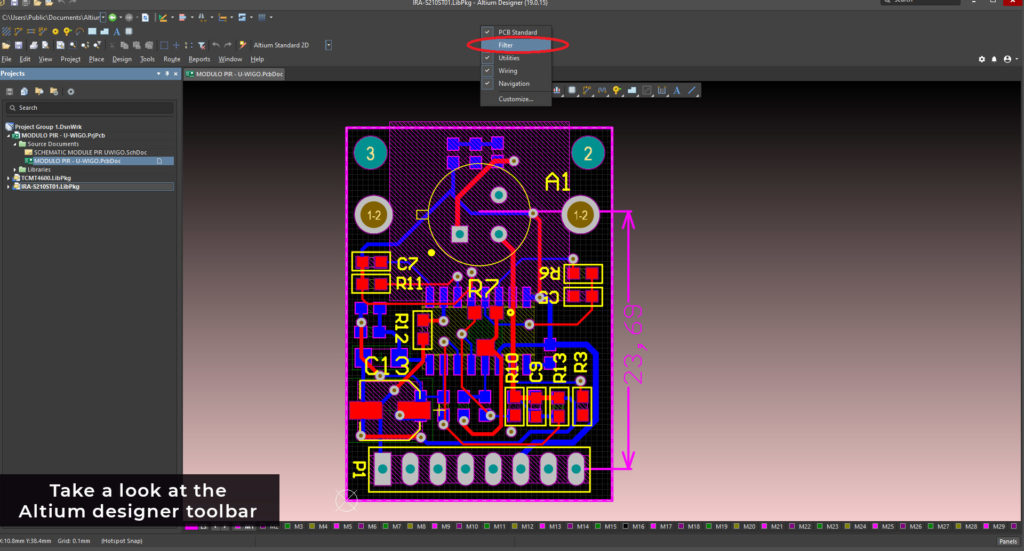
1st. Step: At the top, we can see the Altium toolbar, press right-click to open the available tools, and choose the filter option.
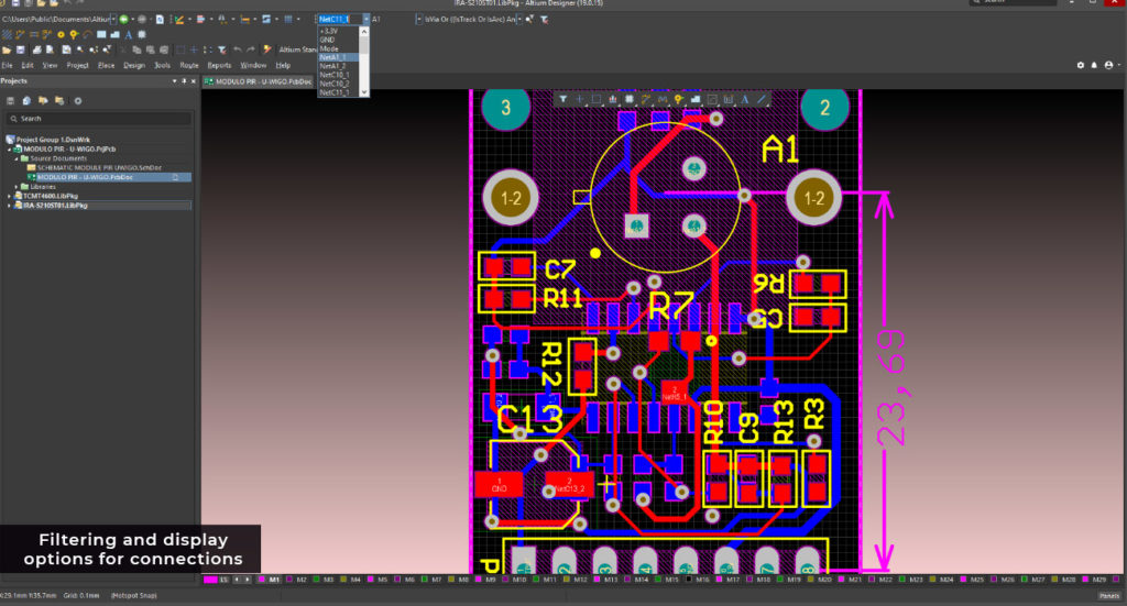
2nd. Step: In this tool, Altium provides us with the first drop-down tab, the list of all the circuit connections, in the next tab a list of all the components included in the schematic diagram, in the third tab we will have a list of functions Specific to filtered for more precise verification
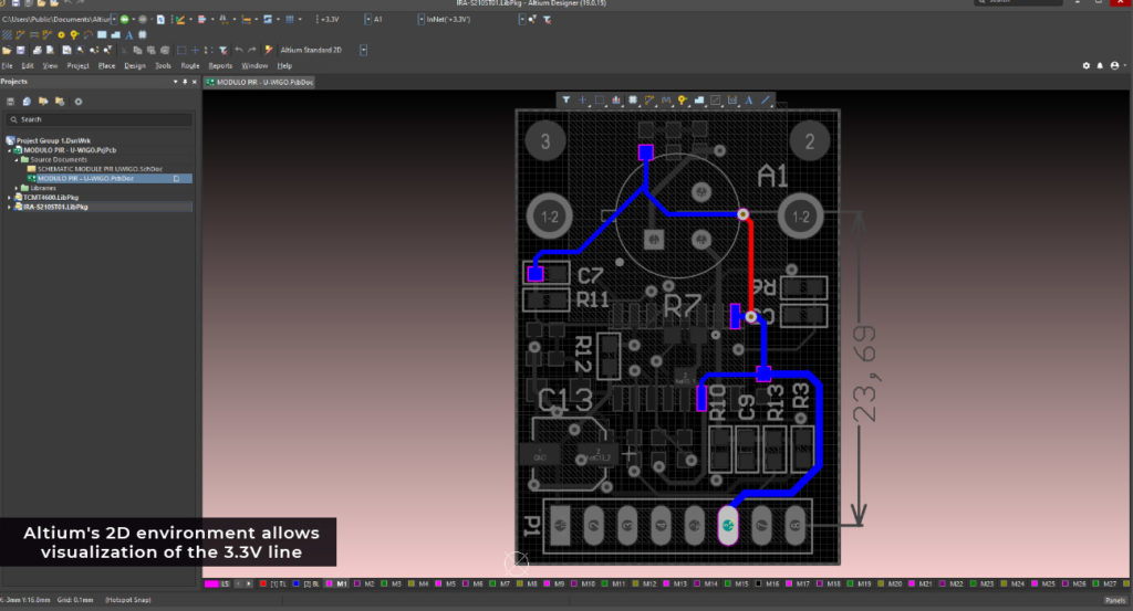
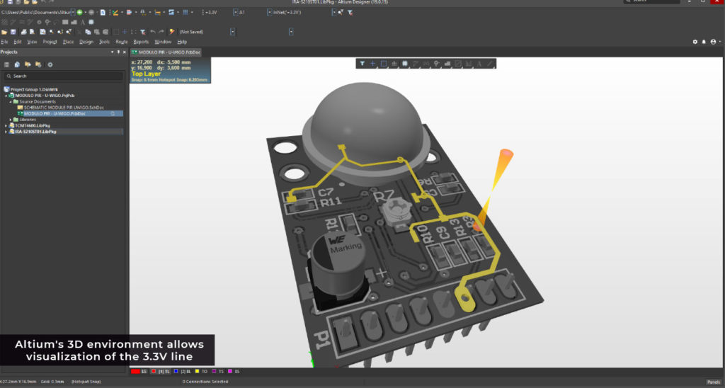
3rd. Step: Finally, we can choose within our filter, the connection or the group of connections that we want to verify, in the following example we will visualize the entire 3.3V power line of our circuit in 2D and 3D, to be able to change the display environments, we press keys 2 and 3.
It is highly relevant to use this tool within the design of printed circuits (PCBs) to give them quality, reliability, and functionality in each of our projects, before going to the manufacturing or production phase.
Posted by

Danilo Ortega – Electronic Engineer