CHALLENGES FOR PCB DESIGNERS ON INDUSTRIAL IOT DESIGNS IN 2020
The word IoT became one of the buzzwords in the technology sector and every day it feels more strongly, with the initiatives of many companies and governments to connect the world, solve problems, facilitate the life of human beings. Over time, the real problems that can be solved by connecting devices begin to become clear, and is possible to identify practical opportunities for innovation and problem-solving.
The ideas for the development and implementation of these technologies often ignore the challenges of the hardware, the economic viability, promising the benefits that can be offered to the world but ignoring the economic part that can be attributed to the development of any IoT project into the future.
These are the factors that you need to take into account in order to create and achieve a successful device:
Multiple wireless protocols.
Communication between devices is one of the most important challenges in the development of new technologies, oppositely, if we had to connect everything in a wired way, choosing a communication protocol for development is not as easy as it is believed, since this Many factors are attributed to it: frequency, data speed, range, interference, etc.
Nowadays in our market, short-range protocols are used, but with better-improved data speed, (WIFI, Bluetooth) and long-range protocols such as LoRa WAN, as the integration of different communication protocols in a single PCB board.

Low consumption design.
In the development of IoT applications, the objective is to optimize consumption to provide environmentally friendly solutions and to reduce the currency factor within what is known as energy consumption, designers must reduce the minimum use of this consumption in the electronic components, eliminating unnecessary functions, using the (“Sleep Mode”) in the sending and receiving data chips, another way is adding energy harvesting methods, such as piezoelectric systems, RF, etc.).
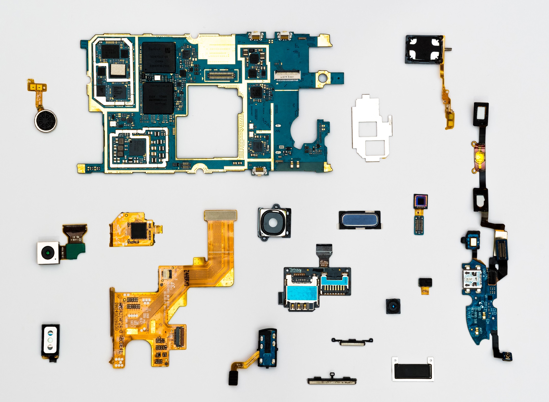
Data processing.
This is one of the most important factors since it will determine the level of complexity and power of the hardware development, or embedded system since it affects the memory level and information processing speed, measurement data, information sending speed, etc.
These were my recommendations obviously each project comes with its own challenges and complexities, the important is to reduce the uncertainty and work through with what has been learned from previous experiences. Each project is an adventure that teaches us and improves our abilities.
Posted by

Danilo Ortega – PCB Designer