PRINTED CIRCUIT DESIGN
Throughout the history of mankind, the development of technology and research has led to the evolution of electronic circuits to a very high level, in several aspects, since the functionality of all technological advances and the creation of devices, have been developed on a printed circuit board (PCB), fundamental role it plays in any technological development or electronic project, to give functionality to it, which is why every day we have more efficient PCB with a wider range of applications for the electronics industry, later we will mention the types and characteristics of PCB, its structure and the whole process involved in the design of a PCB.
What is a pcb
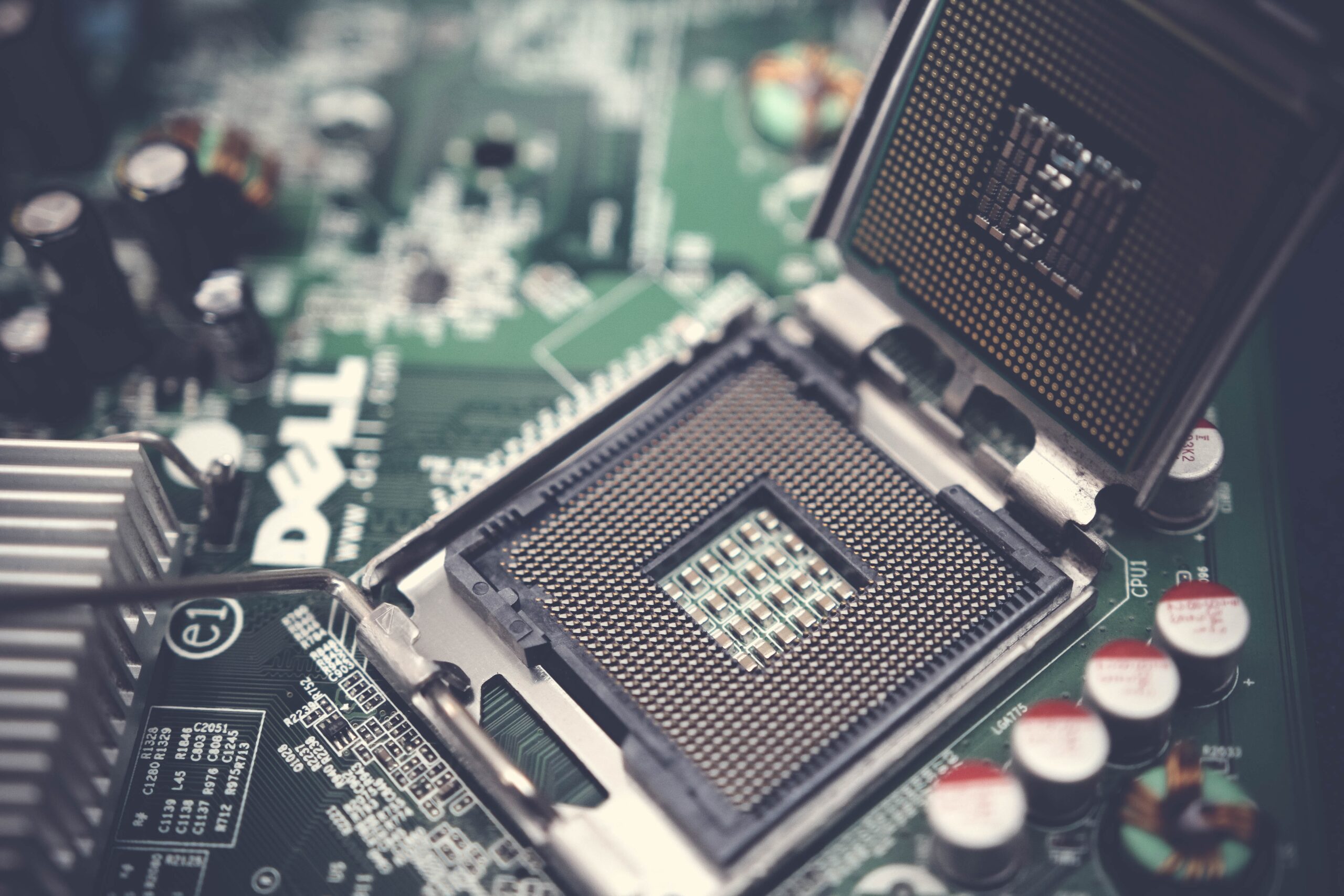
The acronym (PCB) stands for printed circuit board, which has the function of mechanically supporting and electrically interconnecting electrical or electronic components by means of conductive tracks, pads and other features etched from one or more layers of copper foil laminated on and / or between layers of sheets of a non-conductive substrate, called dielectric, the components are usually soldered to the PCB to connect them electrically and mechanically fasten them, where each component has a specific function within the PCB, in order to give functionality, operation to the project being developed.
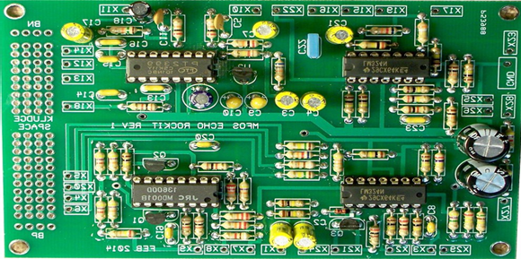
Figure 1. Printed circuit board, (falconer electronics).
Structure of a pcb
In the following figure we can see the main parts that make up a PCB, they are listed and then give an explanation to each of them, the design process has some guidelines that we will see later in volume 2.
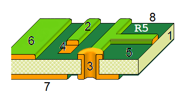
Note that the following are not question numbers, but identifiers from the figure above.
- This session is the dielectric or insulating material between the two copper faces of a PCB, which there are different types of materials, with different thicknesses and dielectric capabilities. Among them the most commonly used: Fiberglass substrate (FR4).
- Trace: The fiberglass substrate of our PCB is laminated with a layer of copper on the top and bottom sides. The thickness of this copper is expressed in terms of weight (in ounces) per square foot. Our boards are manufactured with 1 ounce copper, resulting in a copper thickness of 34 µm. During PCB fabrication, the copper on both sides is selectively etched to form the copper pattern shown in the figure, the traces are the paths that interconnect the assembled components to each other.
- Plated through hole (via): There are a variety of reasons why we need to drill holes in a PCB. For example, you may need to mount a through-hole component or cross a pair of tracks without connecting them electrically. When holes are placed on a PCB, most of the time we plate the sides of the hole with a conductive material so that an electrical signal can pass from the bottom of the hole to the top, in order to get a better chance of interfacing one component to another and to take advantage of the gaps in the design.
- SMT pad or SMT ground: To connect a surface mount component to the PCB, part of the solder mask is removed from each contact point between the component and the PCB. Each of the exposed copper areas is coated with solder that produces a shiny silver surface called a pad or ground. The set of exposed pads associated with a component is called the footprint of the component on the PCB.
- Solder mask: Solder mask is the green (or blue) coating that covers most of the surface of PCBs. It performs three useful functions; it provides a modest level of electrical insulation for the copper it covers, protects the copper from oxidation, and helps prevent solder from adhering to areas you do not want to solder.
- Top copper pouring: only a fraction of the top layer is covered with traces. The unused copper in the top layer is often used in a PCB design by having it carry a supply voltage, in our case 3.3v. Consequently, whenever a device needs power, it will connect to the excess copper in the top layer. The term “pour” is used to evoke the idea that copper is poured onto the PCB in a liquid state, flowing to all available regions that are not occupied by some feature of the PCB.
- Bottom copper pour: the unused region on the underside of the PCB is almost always grounded. This is most often referred to as the “ground plane”. Since many components need to be grounded, there are many holes through the board that connect to the ground plane.
- Silk screen: The silk screen is the white text on the PCB. Generally, the silk screen tells you where to place a component and the value of the components. The part identifiers on the PCB must exactly match the part identifiers on the schematic. [1]
In this section we saw two of the main basic fundamentals of pcb design, later we will be able to see more topics according to the basic fundamentals that will take shape to learn how to design any electronic circuit, for its prototyping and functional projects.
References
[1] Building a development board taken from online: https://inside.mines.edu/~coulston/courses/EENG383/lab/lab01/inlab01.html
Posted by

Danilo Ortega – Electronic Engineer