WHAT IS A SCHEMATIC DESIGN?
Normally all electronic product development processes have guidelines or series of steps that contemplate what is known as R & D, within the product development, we will always find initially having a solid foundation of research, and clear concepts of all product functionality, components to use, technologies, protocols, sensors, power supply etc.; after this we can start a prototyping, this is where the computerized electronic circuit design environment begins, and clearly the initial step is the design of a schematic.
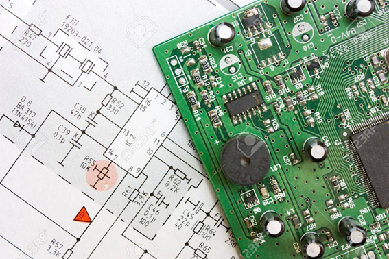
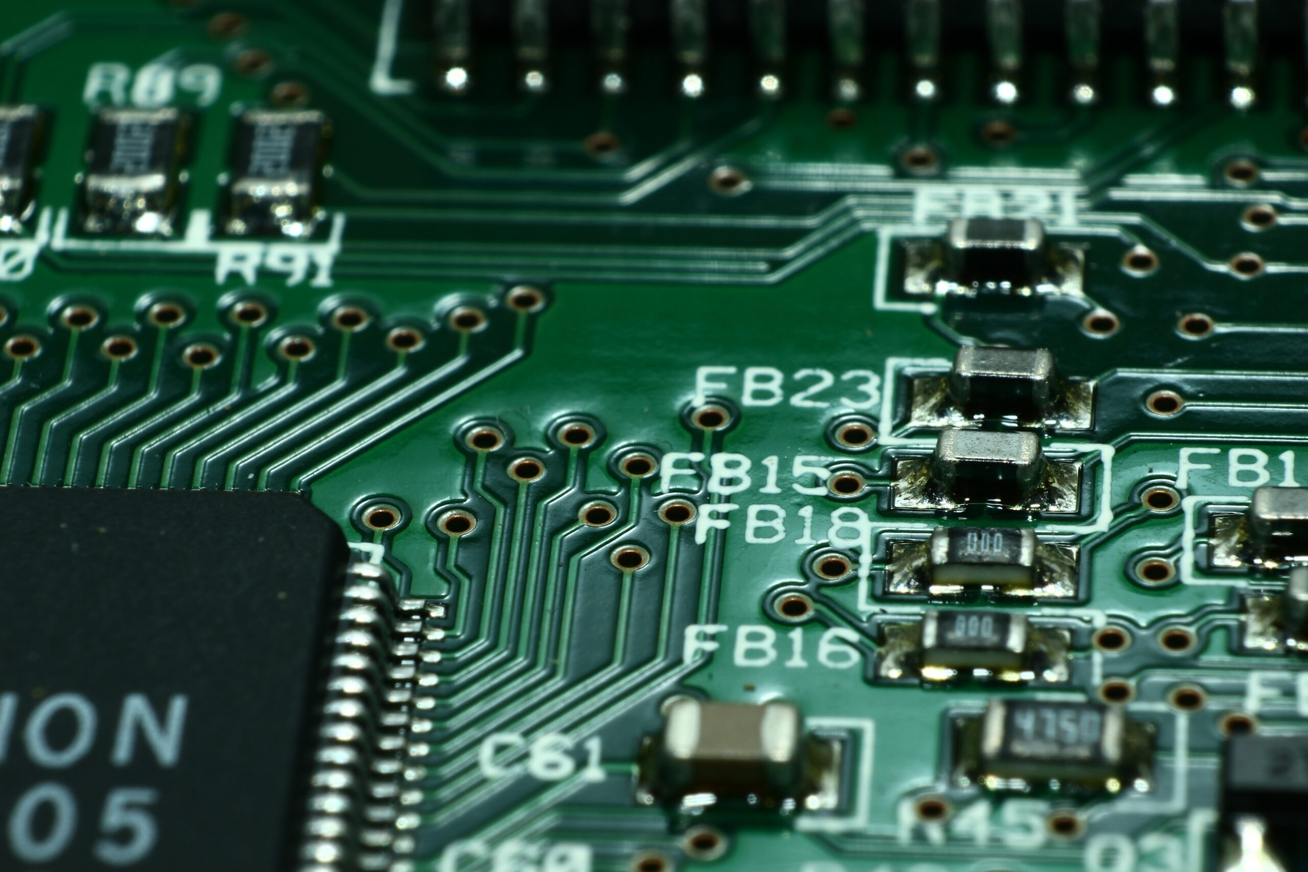
The schematic design or hierarchical design, is a sheet or environment where the different electrical connections of all electronic components that represent the operation of an electronic circuit will be drawn, in which each component is illustrated with symbols and interconnection lines between them; a schematic design is a way to represent an idea; Schematics are drawings or graphics that are used to communicate electronic ideas to others, in short the schematics are a (language) which is universal to represent and share the design ideas and functionality of an electronic circuit.
Within this scheme, the main functional blocks will be represented, such as power supplies, control blocks (microprocessors, controllers, DSP, FPGA,); peripherals or headers for sensor connection, programming ports, ground reference, etc.
Within this topic, a schematic design of an electronic circuit was contextually described in order to understand the environment of a complete development of an electronic product, taking into account the previous topic of electronic design, and the one that will be discussed in the following section.
Posted by

Danilo – Data Science Developer